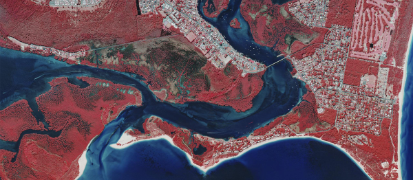
Aerial Imaging
Aerial imaging is one of the most cutting-edge applications in optical technology, leveraging large and super high-resolution sensors essential for various industries. Operating under demanding environmental conditions and across a wide spectral range, it is crucial to eliminate any room for compromise.

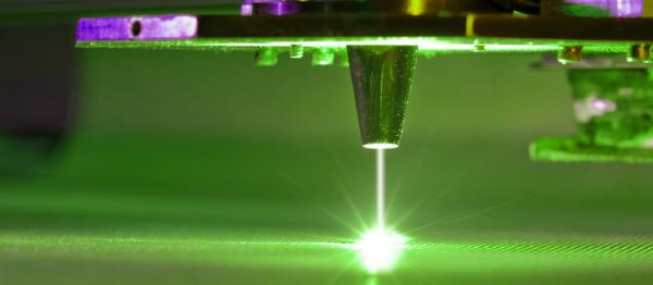
Additive Manufacturing
Not merely a novel means for desktop creation of mechanical parts, 3D printing is poised to revolutionize the future of high-volume manufacturing of complex-shaped parts from a variety of materials.

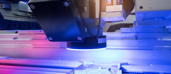
Electronics
Electronics manufacturing require an inspection process with microscope-detail resolution over large areas to ensure quality.
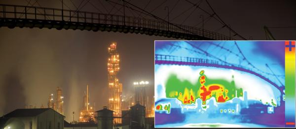
Environmental Monitoring
There are numerous contributors to harmful emissions realeased into our environment including industrial combustion, smelting and metal processing, construction and demolition, and forest fires to name a few.
Laser Industry
Excelitas provides technology that enables powerful lasers used in a wide variety of applications in industrial manufacturing, defense, medicine, and science that require marking, cutting, drilling, heating and welding.

LiDAR and Range Finding
Excelitas has a long and rich history in the field of LiDAR and range finding, from early pioneering work by Dr. McIntyre on Avalanche Photodiodes (APDs) to today’s in-house state of the art manufacturing facilities. We have a proven track record of expertise and accomplishments to help bring next generation designs to life.
Machine Vision and Inspection
Excelitas’ LINOS® and Optem® imaging solutions deliver high-performance, precision imaging for industrial machine vision, semiconductor and electronics inspection, life science imaging, along with other demanding applications. These solutions provide field-proven reliability and exceptionally consistent imaging quality.
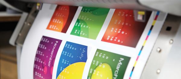
Printing
In printing and publishing, prepress is what occurs between the creation of a print layout and the final printing, including the manufacture of a printing plate.
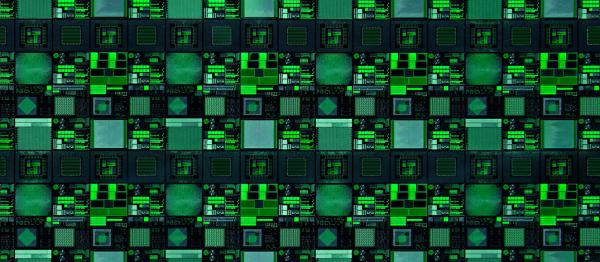
Semiconductor Equipment
The ever-shrinking scale of integrated circuits necessitates higher resolution illumination and imaging for silicon semiconductor production, driving optical systems to extreme ultraviolet wavelengths, better performance, and strict contamination control.